
This is apparently what the front looks like.

Socks outside vs inside
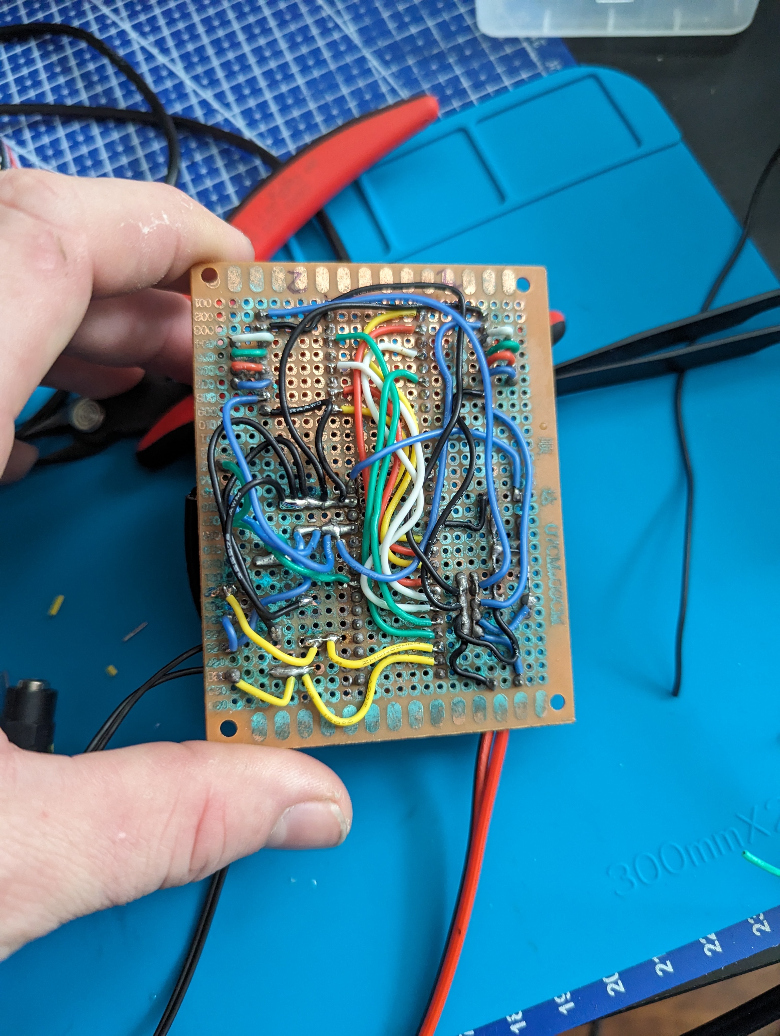
What is it?
Still more reliable than Wayland on nvidia.
also doubles as an electrical fire generator, very versatile
If you are worried about that, then don’t look behind the panel on any computers with a wire wrapped backplane.
The design is very human
Typical spaghetti code
-O2 from the looks of it
Mine almost looks that good
nice
This looks more like the boards they used in the 60s and 70s in prototyping. I have done such a board myself in my youth. All 40xx and 74LSxx DIL chips and a plain dot board. And a sh-tload of patching wire where I had to remove the isolation paint before I could solder that stuff.
I don’t think you could build a working GPU with that wirewrap technology, the frequncies needed are simply to high.
If it’s open, looks don’t matter. Also doesn’t matter if the drivers are trash, or if it runs zero games. It’s all fixable trash - that’s the point.
(Also, that’s not a GPU, but it’s the thought that counts)
What am I looking at?
A free and open source GPU compiled by hands
The free and open source comes with the fact it was hand made ? I don’t get it
Would assume that in this case that the gpu was created and assempled using a open blueprint/schematic thats freely available for anyone to see use and modify. Fairly common thing when it comes to stuff like 3d printing where many people freely share their models for others to use.
The joke is in the eye of the beholder, for me it’s funny because you have the buzzwords “free and open source” which means you can implement it however you want and the user here decided “fuck it, I will do it by hand”.
I don’t get it either
It looks like a wire wrapped prototype board of some kind, impossible to tell the purpose from that photo alone though.
I don’t know, maybe it’s not even a GPU
Looks like an ISA card to me - might be RAM, but I’m not confident at all
Serious response I agree with Pogo, it looks like a handmade RAM.
some pci-e device. but the main chips are probably on the other side of the board.
Haywire. You don’t see that often anymore.
I wonder why
Removed by mod
Judging by the craiglist watermark on the bottom right, it’s probably just a meme listing.
I have stolen it from Chinese website
Why does this look like when i first iterate a pcb and need to bodge the hell out of it to make it work.
You switched two wires.
Dedication to wire this up manually is amazing.
Me when I forget about FPGAs
And the fact that more-than-0-layer PCBs exist
Is there more info about this? I could only find Chinese forums like https://m-weibo-cn.translate.goog/status/OdaBMza1L?from=page_1005052963774131_profile&wvr=6&mod=weibotime&jumpfrom=weibocom
The chips (basic TTL logic, perhaps) are all DIP. This may predate the term “open source”.


